Main Page | Projects IndexGallery Index | Data & Infomation


Building an I2C 4x4 Keypad using a PCF8574 I/O Extender.

Overview

In order to save MCU I/O it is often useful to take advantage of the I2C bus that is available on most modern micro-controllers.

LCD to I2C converters are commonly available on-line but designs or modules intended to connect a keypad to the I2C bus seem to be hard to come by.


A typical I2C to LCD interface module.

For this reason it was decided that a simple keypad interface would be developed that would allow a 4x4 matrix keypad to be accessed via the I2C bus. At the core of this design would be the PCF8574 I/O extender that forms the core of the LCD interface shown above.

Initially an interrupt generating circuit was tested that used a 4017 CMOS IC to scan the matrix of the keypad, this would pause when a key was pressed and the resulting 4 bits of the 4017 and 4 bits from the keypad would be presented to the PCF8574 which would then in tern generate an interrupt.

The interrupt would then prompt the MCU to read the inputs of the PCF8574, decode the result into a pressed key and restart the key-scan via a spare IO pin of the MCU.

Although it worked as a prototype this circuit did suffer from one fatal flaw. As the PCF8574 generates interrupts on transitions of the data presented to its inputs, when the same button was pressed more than once only the first transition would result in an interrupt call to the MCU. In piratical terms this meant that if the numbers 1998 or 2000 were entered into the keypad for example the MCD would only register 198 and 20 as being pressed. 

In the end this approach was abandoned in favor of the more traditional method of using CPU runtime to scan the key matrix over the I2C bus. In the end this proved to be very reliable system that consistently produced good results.

The Circuit


The circuit has been designed to work with one of the cheap matrix keypads commonly available on-line (shown below), these have the following physical connections with 4 lines running to each row and 4 to each column.

As stated above the circuit is centered around a PCF8574 IO extender, programming this device is a little different from usual as there is no direction control register to setup the function of each of the IO pins. Instead a pin is made into an input by simply setting it to logic 1. This then drives the output Hi via an internal constant current source that can be overcome and pulled down to logic 0 through the application of sufficient load on the IO pin.

If the pin is required as an output as long as the internal constant current source is not overcome though excessive loading, sufficient current is available to drive an LED, FET or BJT. However if the pin is required to act as an input all that is needed is to provide sufficient loading in order to pull the pin to a low logic state.

Initially I found this concept unusual but once it was understood what was happening then the following circuit was drawn up.

How it Works


In order for this circuit to function the first four IO lines of the PCF8574 (P0-P3) are used as outputs and the second four (P4-P7) are inputs. As stated earlier to do this a logic 1 must be written to P4-P7 and a logic 0 must be sent to P0-P3. (iomask = &B11110000)

Without the load provided by R5-R8 the outputs of P4-P7 would go into a hi logic state, however with these in place a logic 0 is present on the all 4 lines.

Next to check ROW 0 for a key press the first output of PCF8574 (P0) must be switched on(Row0 = &B00000001)  while maintaining the IO arrangement of the device. This is achieved by sending the iomask patten(&B11110000)combined with the Row0 pattern(&B00000001) to the device (&B11110001).

If this is done Row 0 will be in a logic 1 state and Rows 2-4 will be at logic 0 at the same time because of R5-R7, P4-P7 will also be in a low logic state.

If however any of the keys on Row 0 are pressed during this time, the current provided by output P0 and R1 will make its way down to one of the column inputs P4-P7 depending on the which of the keys being pressed.

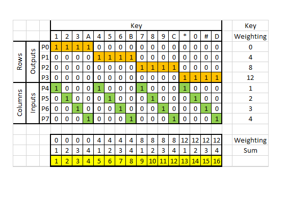
This is shown graphically below where the keys 1,2,3 or A corresponding to an input on P4,P5,P6 or P7. The process is then repeated for all the other rows in order to check for a pressed key.

To make decoding easier weighting is applied to each of the energised rows and the activated columns, for example if 9 is pressed P2 with a weighting of 8 and P6 with a weighting of 3 will both be activated at the same time. If these are added together 8+3 = 11 the 11th entry of a lookup table can be used to hold the corresponding key value. This system is used in the example MicroMite program described later.
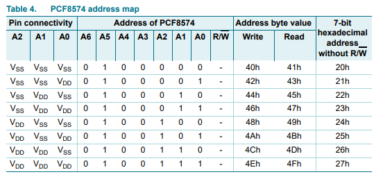
Within the design 3 links are also provided in order to select the address of the I2C keyboard upon the bus. The design uses an PCF8574 which, according to the data sheet, with the AO link made  should respond to an address of H&21.
The I2C bus connection, with the exception on the INT output has been made the same as the I2C bus of LCD converter mentioned above to make connection easier.

Finally for this design a supply of 5V has been used in which a 100nf capacitor is used for suppression, as I am using this with a MicroMite controller the bus is 5V tolerant so this should not pose a problem in the long term. As it stands however I am not sure if this would be a problem anyway as the design dose not have any local pull ups to the +5V rail, instead pull ups are only present on the MicroMite board to the local 3.3V supply.


Construction

The strip board layout shown below is fairly compact with only a small number of track cuts being required, the hardest cuts are the gaps in between the address selection jumpers. If you will not be regularly changing the address then these links can be left out and the individual address pins can be hard wired to either supply or ground, in order to permanently select the desired address.

This is the as built layout with the essential mounting points drilled and ready for use. I have used a 90 degree 0.1" edge connector for the keypad as this facilitates connection if it is mounted on the reverse side of the front panel of the intended project.With the exception if the interrupt pin this board is pin compatible with the LCD  I2C interface board shown at the beginning of this page.


MicroMite Test and Library Program

In order to test and evaluate the circuit a program was developed for the MicroMite operating system, as it stands this is set to communicate with the keyboard at address 21H on the bus. The program is written in the form of a Library so that it can be pasted into the bottom of an existing program and called in order to set up communications and to access the board during normal operation.

If this program is download and ran, then each pressed key will be displayed on the serial console to the PC.


Links:

Click here to download the associated project files:

- Circuit Diagram

- Strpboard Layout

MMCODE